Common Basic Concept in PCB Design
2021-09-22
1. FR4
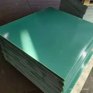
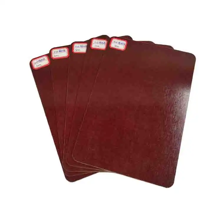
FR4 sheet is a glass fiber epoxy resin coating plate, a substrate in a circuit board, which can be divided into general FR4 plates and high Tg FR4 sheets, and Tg is a glass conversion temperature, i.e., melting point. The circuit board must be flame-resistant and cannot be burned at a certain temperature, only can be soften. At this time, the temperature point is called the glass transformation temperature (TG point), which is related to the size stability of the PCB board.
|
General Tg's sheet is 130 degrees, high Tg is generally greater than 170 degrees, medium Tg is more than 150 degrees. Usually the PCB printed plate of Tg ≥ 110 ° C, referred to as a high TG printing plate. The Tg of the substrate is improved, the heat resistance, moisture resistance, chemical resistance, and stability of the printed plate increases and improves. The higher the TG value, the better the temperature resistance of the sheet, especially in the lead-free process, and the high TG application is more.
Material | TG | MOT |
FR4 General TG | 130 ° C | 110 ° C |
FR4 Medium TG | 150 ° C | 130 ° C |
FR4 High TG | 170 ° C | 150 ° C |
Polyimide Super High TG | 260 ° C | 240 ° C |
2. Impedance Matching
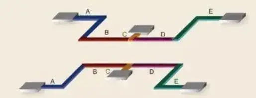
Impedance matching is mainly used for transmission lines to achieve all high-frequency microwave signals can be transmitted to the purpose of the load point, and there is almost no signal reflecting back source, thereby improving energy efficiency. The signal source internal resistance is equal to the characteristic impedance of the transmitted transmission line, or the characteristic impedance of the transmission line is equal to the size of the load impedance, and the input terminal or output of the transmission line is called the input or output terminal, referred to as Impedance matching. The common impedance control values in the PCB include: 100 ohm differential impedance, 90 ohm differential impedance, and single-ended 50 ohm impedance.
|
3. Surface Treatment
PCB board surface treatment is generally divided into several, in order to better understand the problems of their PCB design, simple introduction:
1) Spraying
Spraying is the most common surface treatment process in the circuit board, which has good weldability and can be used in most electronics. Spray plates to other surface treatments, it is costly and weldable advantages; the deficiencies is that there is no flat gold flat, especially when the large-scale window is opened, and the phenomenon of tin is not flat.
2) Shen Xi
Shen Xi and sprayed tin is different in its flatness, but the deficiencies are extremely easy to oxidize.
3) Shenjin
As long as it is "sink" its flatness is better than "spray". Shenjin is lead-free, Shenjin is generally used for gold fingers, press the keyboard, because the resistance of the gold is small, so the contact must be used to use the button, such as the button on the phone. Shenjin is a soft gold. For the use of gold plated for frequent plugging, Shenjin is mainly Shenjin.
4) Gold plating
Gold plating, gold plating has poor welding, but its hardness is better than Shenjin when it has been mentioned in Shenjin. In the design of MID and VR, there is generally no such process
Small assistant Tip: If there is a need for flatness, such as impedance circuit boards (such as microstrip lines) that require frequencies, as far as the gold process is used; generally, with BGA's MID boards use the Shenjin process.
5) OSP
It mainly relies on the reaction between the drug and welded copper skin to produce weldability, the only advantage is fast, low cost; but due to poor weldability, it is easy to oxidize, and the circuit board line is generally used.
4. Core / PP film (semi-cured film)
The reinforcing material is immersed in a resin, one or two sides with a copper foil, a plate-like material formed by hot pressing, called a copper cladding plate. It is the basic material of PCB, often called substrates. When it is used for multi-layers, it is also called the core board (Core)
A sheet-like bonding material synthesized by a resin and carrier is referred to as a PP sheet.
The core panel and semi-solid tablets are common materials for making pressing multilayers.
5. Differential Line
The differential signal is that the drive end sends two equivalents, inverted signals, and the receiving end determines "0" or "1" by comparing the difference between the two voltages. The pair of traces that carry differential signals is called differential traces. Differential signals, some also known as the differential signal, transmitted all the way to the two signals, depending on the signal, depending on the two signal level differences. In order to ensure that the two signals are identical, keep parallel, line width, and line spacing when wiring.
|
6. Signal Integrity
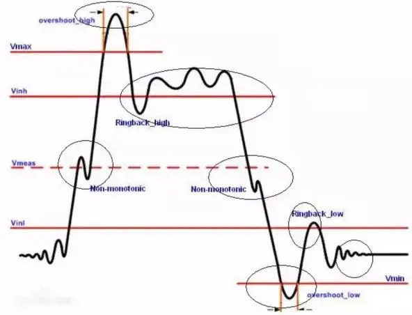
Signal integrity refers to the quality of the signal on the transmission line. The signal has a good signal integrity to refer to the value of the voltage level required to be reached when needed. Different signal integrity is not caused by a single factor, but a variety of factors in board-level design. The main signal integrity problems include reflection, oscillation, bullet, crosstalk, and the like.
7. Signal Reflection
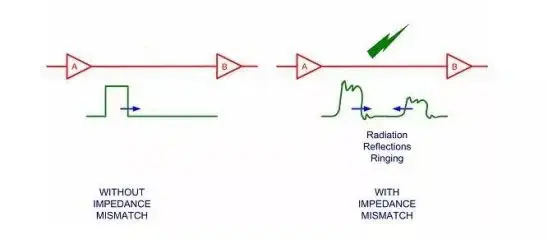
Reflection is echo on the transmission line. A portion of the signal power (voltage and current) is transmitted to the line and reaches the load, but some are reflected. If the source is the same impedance with the load end, the reflection does not happen. The source and load-end impedance mismatch can cause the line to reflect on the line, and the load reflects a part of the voltage back to the source. If the load impedance is smaller than the source impedance, the reflected voltage is negative, that is, if the load impedance is greater than the source impedance, the reflected voltage is positive. The geometry of the wiring, incorrect linear connection, the change in the transfer of the connector and the discontinuous discontinuous power supply plane can cause such reflection.
Reflection can cause signal to overshoot, downhest undershoot, ring ringing, side edge slide is the step voltage wave.
|
8. Crosstalk
Cross is the coupling between the two signal lines, the mutual feelings between the signal lines, and the noise caused by the line. Capacitive coupling initiates a coupling current while inductive coupling initiates a coupling voltage. The parameters of the PCB plate, the electrical characteristics of the signal line spacing, the driving end, and the receiving end, and the linear end of the line have a certain impact on crosstalk.
9. Internal Electrical Layer
The internal layer is a negative sheet of the PCB, and the main function is to perform power segmentation as a layer of power or ground.
10. Blind Hole
Blind hole: extends from the intermediate layer to a via hole in a surface layer of the PCB. Common, there is a first-order, second-order, such as a first-order blind hole refers to a hyperthermole of the second layer to the TOP layer or the diamonds of the second layer to Bottom.
Buried hole: from a via between one middle to another, it does not extend to the surface layer of the PCB.
11. Test Point
Generally referring to a separate PTH hole, SMT pad, gold finger, bonding finger, IC finger, BGA welding point, and test points for customers after the plug-in.
12. Mark
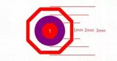
The MARK point is the position identification point of the PCB applied to the automatic postal machine in the board design, also known as the optical point. The choice of Mark Point Directly affects the patch efficiency of the automatic postmaker. The selection of the general MARK point is related to the model of the automatic postmaker. The MARK point is generally designed to ф1 mm (40 mil) circular graphics. Taking into account the contrast of the material color and the environment, there is no resistant welding than the optical positioning reference symbol large 0.5 mm (19.7 mil), nor does any character, see the figure. The optical positioning reference symbol on the same panel is the same as its adjacent inner layer, that is, there is a copper foil in three reference symbols. The isolated optical positioning symbol around 10mm unparalleled wire should be designed with a protective ring having an inner diameter of 2mm width of 1 mm, and an 8-sided isolation copper ring having a vertical diameter of 2.8 mm is around.
|
13. PTH (metallized hole) / nPth (non-metallized hole)
The hole in the hole wall is deposited as a metallized hole, which is mainly used for electrical connection of interlayer electrically conductive patterns. Conversely, it is non-metallic aperture, generally used as a positioning hole or mounting hole.

