Why is the Common PCB Plate Thickness is 1.6mm
2021-12-14
The general PCB finished plate thickness is 0.8mm to 1.6.mm between 1.6.mm, and the more common plate thickness specification is designed according to the 1.6 mm of the metric unit (about 63mil), many plugins The standard is also adapted in accordance with 1.6mm, what is the 1.6mm thickness standard?
We learned that the "PCB Development History" chapter of the "PCB development history" is designed by the PCB design. In the era of tubes, the PCB industry is still in the sprouting stage. Since the amount of heat generated by the tube component is large, the volume is bulky, it is inconvenient to install on the printed circuit board (Need a certain mechanical strength), the production of electronic products at the time was basically a handmade studio installation. Of course, this is also related to the development of the substrate material of the PCB, as the epoxy resin of the PCB substrate (see the PCB of the column) This chapter of the substrate resin), the manufacturing technology of the PCB substrate, copper foil, etc. have not been commercialized.
In the 1920s, circuit developers used electric wood (phenolic resins), gypsum board, cardboard, and even thin wood-building circuit boards (forms similar to the cave plate or breadboard, with a printed circuit board). They drill on the material and then securely secure the flat copper wire to the board to form an interconnected circuit with a rivet or bolt.
Among them, electric wood is also a phenolic resin, from German chemist Adolf Von Bayer (1835-1917) first synthesized in 1872. In 1907, the American Chemist (1863-1944) was born in Belgium (1863-1944) improved the production technology of phenolic resin, and the resin was practiced, industrialized. In 1910, he established a general Bakelite and uses the name "Bakelite" "Bakelite" to the phenolic resin trademark according to his own name.
At the beginning of the 20th century, relying on Bakeland's phenolic resin manufacturing patents, in Germany, United Kingdom, France and Japan and other countries, the industrial production of phenolic resins has been achieved. Phenolic resins also begin to be widely used in the knobs of the radio, turntable, mounting components (non-printed circuit boards), and even radios.
In 1921, the laminate manufactured by Formica has been integrated into the manufacturing of household radio and marine radio. In 1927, Formica found that the formation of decorative paper was added to the printing process, and their laminate can be made into a simulated wood grain. And marble pattern. As the laminated plate becomes more colorful and decorative, its market has expanded rapidly. At that time, there were a phenolic laminate as a decorative panel of the table surface.
Phenolic laminate is a rugged and well-insulated polymer material with heat, waterproof, chemical resistance and can withstand the characteristics of high current. Although it is not specially developed as a circuit board, more widely used in decoration Due to the use of panels, the phenolic laminate is much better as the mounting support of the tube or as the mounting of the tube, and there is a lot of strength relative to the plasterboard, the cardboard, or the thin wood flakes, and the phenolic laminate is used instead of cardboard or thin wooden board as a circuit. The board is natural and there is a natural thing.
However, in the phenolic laminate, the phenolic laminate is punched and then connecting all electronic components. It is still a very laborious thing. It is better than playing the cave board. After all, the cave board is still pre-tied. Not long, some people came up with a method, stick a copper foil on the phenolic laminate, and then etched the interconnected line between the components on the copper foil (1913, Berry in the United Kingdom invented the resist The agent is applied to the metal foil, and the etch is not coated, thereby forming a conductive pattern, which is made a single-sided printed circuit board. Soon, the development of the interconnection system between multiple boards produces the relevant needs of the panel connector.
At the time of 1/16 inches or 63 mil, the production thickness of the phenolic laminate at that time, the panel panel connector is naturally designed according to the thickness of 1/16 inches (about 63 mil or 1.6 mm), which forms a supporting Industrial chains, 1/16 inches (about 63 mil or 1.6mm) thickness also forms a default standard for industry.
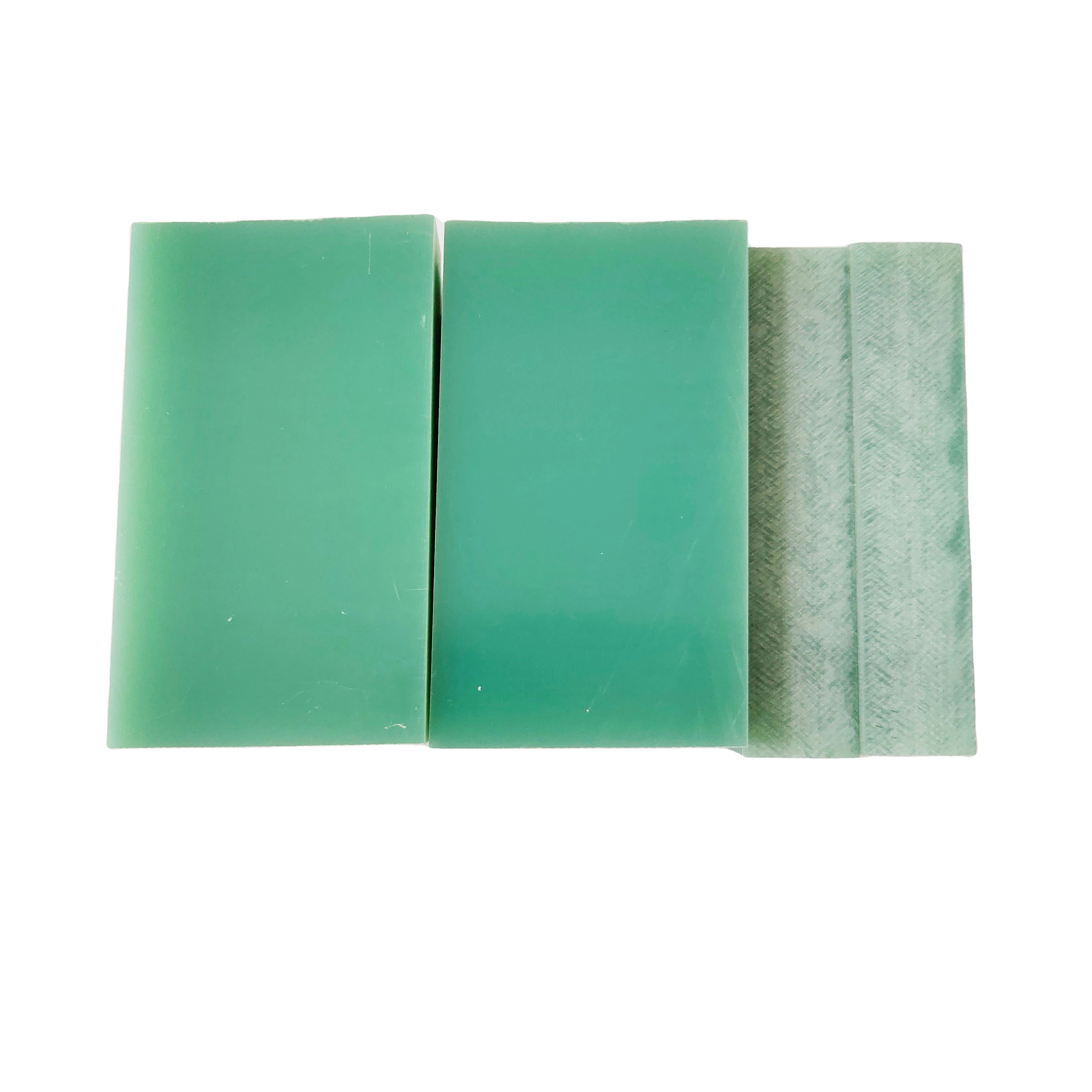
Today, the development of the substrate material has been very diverse such as FR4 sheet, but 1.6mm (or 63mil of the British unit) is still the default molded plate thickness of the PCB board factory, but the standard plate thickness range is extended to 0.8mm to 1.6mm. (Specifically based on the process of board factory, some plate factory is 0.6mm ~ 2.5mm)
Of course, if the PCB to produce thinner or thicker (such as 20 layers) is also possible, such as 0.4 mm or 3.0 mm, but require additional payboard costs, it needs to be considered when the PCB is designed.
When determining the PCB thickness, there is a need to consider many design and manufacture factors, such as:
Copper thickness
Plate
PCB layer number
signal type
Type of through holes
Operating environment
Manufactured factors affecting the thickness of the PCB include:
Craft capabilities for drilling equipment
Copper thickness
Layer number
Division method
Factors that need to be considered for PCB design of non-standard thickness:
1. Plate factory's process capacity
The first thing to consider is that your board factory has equipment to make the thickness you need. This decision should be made as soon as possible while considering other relevant DFM design requirements. Otherwise, you may be forced to modify and redesign your PCB laminated structure.
2. Extend delivery time
If the board is selected is not a standing material, it is often extended to the production cycle of the PCB, so it is necessary to consider delivery time for non-standard plate thickness.
3. Additional fees
This may be the most important point, you need to assess the cost of special sheets, additional manufacturing costs, and time cost extending to determine whether additional cost is acceptable.
Priority adopts a standard PCB thickness will make your board make faster and lower cost. However, if you decide to choose a non-standard thickness, you should communicate with the board factory before starting the PCB design, ensuring that the process can be manufactured and communicated during delivery and additional manufacturing costs.


