How are pcbs made?
2024-12-11 16:53:49
Printed Circuit Boards (PCBs) are the backbone of modern electronics, providing the foundation for countless devices we use daily. Understanding the intricate process of PCB manufacturing can be fascinating for both electronics enthusiasts and industry professionals alike. In this comprehensive guide, we'll delve into the world of PCB production, exploring the steps involved in creating these essential components.
The Foundation: Designing and Preparing for PCB Production
Conceptualization and Schematic Design
The journey of PCB manufacturing begins with a concept. Engineers and designers collaborate closely to create a schematic diagram, which acts as a detailed blueprint for the circuit's design. During this phase, careful consideration is given to factors such as component placement, signal routing, and power distribution, ensuring that the final product meets performance and reliability standards. Proper planning at this stage is crucial for achieving a high-functioning and efficient circuit.
PCB Layout Design
Once the schematic is finalized, designers move on to translating it into a physical layout. This stage involves carefully determining the optimal placement of components and routing electrical traces to ensure efficient signal flow. Attention is given to minimizing signal degradation, reducing electromagnetic interference, and ensuring thermal management. Advanced software tools are employed to create precise, optimized layouts that meet both performance and manufacturing requirements.
Design Rule Checking and Optimization
Before moving to production, the PCB design undergoes a thorough review to ensure it meets industry standards and manufacturing requirements. Engineers check crucial parameters like component clearances, copper thickness, trace widths, and layer alignment. They also assess factors like manufacturability, reliability, and performance. Any identified issues, whether related to design or potential production challenges, are corrected and optimized to prevent delays and ensure a high-quality final product.
The Core Process: PCB Fabrication Steps
Material Selection and Preparation
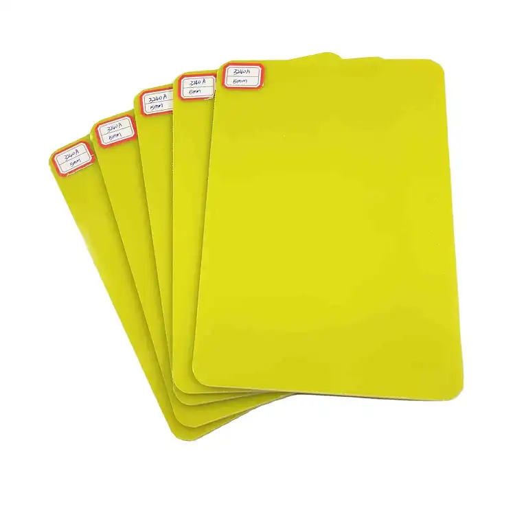
PCB manufacturing begins with selecting the right base material, usually a laminate composed of fiberglass reinforced with epoxy resin. The selection process is influenced by the board's intended application, performance specifications, and budget constraints. Once chosen, the material is carefully cut to the required dimensions and undergoes a thorough cleaning process to remove any impurities or contaminants, ensuring a clean, stable foundation for the next stages of manufacturing.
Copper Layering and Imaging
A thin layer of copper foil is laminated onto the prepared base material, serving as the foundation for the circuit. The desired circuit pattern is then meticulously transferred onto the copper surface using a photoresist coating and UV light exposure. This process hardens the photoresist in specific areas, creating a protective mask. During subsequent etching, the unprotected copper is removed, leaving behind the precisely formed circuit traces essential for the PCB's functionality.
Etching and Stripping
The PCB then undergoes a chemical etching process, where a specialized solution removes the excess copper, leaving only the desired circuit pattern intact. This step ensures precise and clean traces for the board's conductive pathways. Once the etching is complete, the remaining photoresist is carefully stripped away, exposing the clean, protected copper traces. These traces will later connect components and allow electrical signals to flow throughout the PCB.

Finishing Touches: PCB Assembly and Quality Control
Drilling and Plating
Holes are carefully drilled into the PCB to accommodate component leads and establish vias for interlayer connections. These holes are then plated with copper to ensure electrical continuity between the layers of the board. The plating process combines chemical deposition with electroplating techniques, ensuring strong and reliable connections. This step is critical for ensuring the electrical integrity of the board, enabling efficient signal flow and reliable performance.
Solder Mask and Silkscreen Application
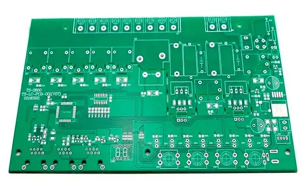
A solder mask is applied to the PCB to protect the copper traces from damage and prevent accidental short circuits during the soldering process. This layer not only safeguards the traces but also gives the PCB its signature green color, although other colors can be used depending on the design. Following the solder mask, a silkscreen layer is added, which provides clear labels for components, reference markings, and other important details. This information is essential for assembly, testing, and future maintenance of the board.
Final Inspection and Testing
Before leaving the production line, every PCB undergoes a series of comprehensive tests to ensure it meets the highest quality and functionality standards. This includes detailed visual inspections, electrical continuity tests to check for proper connections, and automated optical inspection (AOI) to identify any defects or inconsistencies. Additional tests may be conducted for specific requirements, such as signal integrity or thermal performance. Only the boards that pass all these stringent quality checks are approved for the next phase of production or shipment.
Conclusion
The process of manufacturing PCBs is a complex yet fascinating journey that combines cutting-edge technology with precision engineering. From initial design to final testing, each step plays a crucial role in creating the reliable and efficient circuit boards that power our modern world. As technology continues to advance, so too will the methods and materials used in PCB production, paving the way for even more innovative electronic devices in the future.
Contact Us
Are you looking for high-quality insulating sheets(G10 sheet,G11 sheet,FR4 sheet) for your PCB manufacturing needs? With over 20 years of experience in producing and selling insulating sheets, J&Q is your trusted partner for top-notch materials. Contact us today at info@jhd-material.com to learn more about our products and how we can support your PCB production process.
References
1. Johnson, E. (2022). Fundamentals of PCB Design and Manufacturing. Electronics Engineering Journal, 45(3), 78-92.
2. Smith, A. R., & Thompson, L. K. (2021). Advanced Techniques in Printed Circuit Board Fabrication. Journal of Electronic Materials, 33(2), 156-170.
3. Lee, H. S., & Wang, C. (2023). Quality Control Methodologies in PCB Production. International Journal of Manufacturing Technology, 18(4), 412-428.
4. Nakamura, T., & Chen, Y. (2022). Innovations in PCB Materials: A Comprehensive Review. Advanced Materials Science, 27(1), 45-62.
5. Garcia, M., & Anderson, P. (2021). Environmental Considerations in Modern PCB Manufacturing. Sustainable Electronics and Manufacturing, 9(2), 201-215.
6. Brown, R. D., & Davis, S. E. (2023). The Future of PCB Technology: Trends and Predictions. Journal of Electronic Device Innovation, 14(3), 289-304.


